ASTR 511 (O'Connell) Lecture Notes
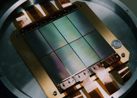
Subaru CCD Mosaic 8 x (2k x 4k)
I. REFERENCES FOR CCD'S
General
- Buil, CCD Astronomy
- Howell, Handbook of CCD Astronomy
- Kitchin, Astrophysical Techniques
- Rieke, Detection of Light : general introduction to detector physics
- LLM Sec. 7.3.3.
-
MacKay, Ann Rev Astr Ap, 24, 255, 1986 "CCDs in Astronomy" (review)
- Timothy, PASP, 95, 810, 1983: discussion of many detector types
CCD Data Reduction and Applications
-
Abbott, "In
Situ CCD Testing"
- Massey, A User's Guide to CCD
Reductions with IRAF (1997)
- Craig & Chambers
(Astropy), CCD
Data Reduction Guide (Python)
- Tyson,
JOSAA, 3, 2131, 1986: high precision technique
-
Hook & Fruchter, "Dithering, Sampling and Image Reconstruction";
also see
the HST
DrizzlePak Handbook.
- Stetson,
PASP, 106, 250, 1994 and references therein. Widely-used ALLFRAME
and DAOPHOT point-source CCD photometry programs.
-
Franx et al. AJ, 98, 538, 1989: sample application to
surface photometry
- Bertin & Arnouts, A&AS, 317, 393, 1996 SExtractor---source ID and extraction software for digital images. Obtain software here.
II. GENERAL DETECTOR CHARACTERIZATION
QUANTUM EFFICIENCY |

Schematic QE curves for various classes of detector |
- "Detective quantum efficiency" is defined to be [(SNRout)/(SNRin)]2, where SNR is the signal-to-noise ratio and "in" and "out" refer to the input and output signals to/from the detector, respectively. DQE combines basic QE with the noise introduced by the detector. This quantity is really what matters in comparing detectors, but it is so dependent on specific details of operations/applications that it is rarely used.
- Wavelength region over which QE is sufficient for operation
- Definition: ratio of maximum to minimum measurable signal
- E.g. maximum number of events in a CCD pixel is determined by photoelectron "full well" capacity or digitization maximum (typically 2 bytes); minimum is determined by dark current/readout noise
- Applies to a single exposure; effective dynamic range can be increased with multiple exposures
- Typical values: 100 (Pg); 104 (CCD); 105 (PMT)
- Related concepts:
- Linear Range: range of signals for which [Output] = k x [Input], where k is a constant. Generally smaller than the calibrateable range
- Threshold: minimum measurable signal. Influenced by detector noise or other intrinsic characteristics (e.g. fog on Pg plates)
- Saturation point: level where detector response ceases to increase with the signal
- Temporal
- PMT: ~0.0001 ms
- CCD: ~10 ms per pixel
- PMT: ~0.0001 ms
- Spatial (array detectors)
- Pixel = minimum measureable area of detector surface. Typically 10-50 µ on Pg or semiconductor types. Pixels are not necessarily independent of one another.
- Resolution cell: according to the Nyquist criterion, the
resolution cell is 2x the size of the minimum
independent measurable area. For proper sampling of an image,
we need at least 2 pixels per resolution cell, but in practice there
may be many more. A lower pixel density implies "undersampled"
imaging. A significantly higher pixel density does not provide more
information and is a waste of pixels.
-
For best pixel matching in an imaging application, the Nyquist
criterion implies that 1 pixel should span ~ (FWHM)/2, where FWHM is
the full width half maximum of the point spread function.
- Spectral
- Most UVOIR detectors are broad-band and have inherently poor spectral resolution. One must use external elements (filters, gratings, photonics) to provide spectral resolution
- Exception: superconducting "3D" detectors, which measure photon energy as well as position; current spectral resolution is R ~ 100
SPECTRAL RANGE
DYNAMIC RANGE
NOISE CHARACTERISTICS
-
See discussion of various types of detector noise in
Lecture 7 notes
RESOLUTION
III. BRIEF HISTORY OF ASTRONOMICAL DETECTORS
PHOTOGRAPHIC ASTRONOMY:
-
Photographic emulsions work by storing in AgBr crystals the
photoelectrons ejected following absorption of photons during exposure
to light. Chemical reactions during development cause the crystals to
precipitate grains of silver, which form a permanent image.
Film was the detector of choice for most applications in astronomy
from around 1900 to 1950 and for imaging until about 1980. It is
impossible to exaggerate its importance to the development of modern
astronomy. Even with relatively low QE, photographic plates
offered decisive advantages over visual observations:
- Very long exposure times (up to a week in early applications),
meaning limiting fluxes thousands of times fainter
- A permanent,
objective record of astronomical images and spectra
- Geometric stability -- important for astrometry and morphology
- Large formats for wide field surveys
- Extension of observations to EM bands beyond the "visual" band. The classic "photographic" band is centered around 4500 Å. Astronomical photography ultimately covered the range 3200-10000 Å.
- It is relatively insensitive,
with QE ~ 1%.
- Pg materials have non-negligible thresholds (a minimum of ~4
photoelectrons per grain). "Reciprocity failure" refers to the fact
that the threshold exposure must be delivered within a certain
critical time period or the photoelectrons on a grain will be
lost.
- Pg materials have a strongly non-linear response function,
and limited dynamic range.
- These properties plus the use of
hard-to-control chemical processes for emulsion deposition &
development makes them very difficult to calibrate
quantitatively.
- Each individual plate (or at the best, each co-processed "batch" of
plates) has different response characteristics.
- Conversion of data to quantitative form (e.g. with microdensitometers) is slow and cumbersome.
PHOTOELECTRIC ASTRONOMY TO 1980:
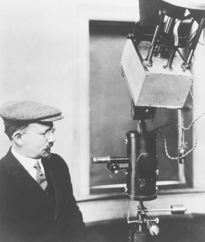
-
In 1907, Joel
Stebbins (UIll, UWisc) began testing various types
of photoelectronic detectors. These, such as selenium
phototubes, were largely experimental and temperamental, but use of PE
devices spread after the 1920's. World War II greatly accelerated
these technologies, with mass production of high quality vacuum tubes
and sensitive electronics for detection of faint signals.
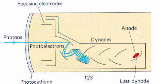
The key design for astronomy was the
photomultiplier
tube (PMT), the first widely used example of which was the RCA
1P21. The initial detector in a PMT is a photo-emissive
cathode surface, made from alkali metal compounds, which ejects a
single electron in response to a photon absorption. A series of other
"secondary electron emissive" surfaces (the "dynode chain") amplifies
this into a burst of ~106-7 electrons and deposits this on
an anode. (See illustration below.)
- Most of these employ some type
of image
intensifier vacuum tube as a key element. This technology was
developed for military night vision systems. Intensifiers produce
easily detectable light pulses in a 2-D image field from individual
incident photons by accelerating the photo-electrons to high energies
and/or producing a cascade of electrons, then focussing these on a
luminescent output screen. Disadvantages include the frequent use of
high voltages (e.g. 25 kV) and serious image blur which, however, can
be reduced by the use of pulse centroiding electronics. Fiber
optic input/output plates were commonly used with intensifiers after
1970.
Microchannel
plate (MCP) intensifiers have often been used in space astronomy
missions (including HST, GALEX, and FUSE).
SOLID STATE ARRAY DETECTORS
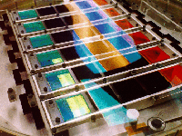
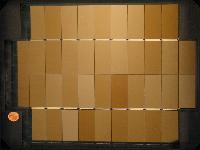
-
But by far the most successful 2-D devices for astronomy emerging in
the last 50 years have been solid
state, semiconductor arrays. These are based on
photo-conductive materials fabricated with embedded
microelectronic integrated circuits on thin wafers
by photolithography.
Although lower quality devices can be mass-produced by microchip
"foundries," professional grade detectors still need to be
custom-processed.
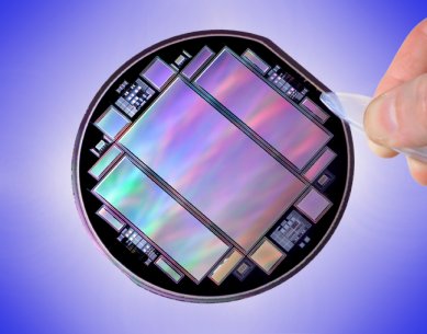
The image at the right shows a wafer containing a number
of co-fabricated CCDs and other devices.
Solid state arrays are now employed as astronomical detectors from the
X-ray to the far-infrared. The most widely used is
the Charge-Coupled
Device (CCD), which operates at wavelengths from the X-ray to
~1 µ. CCD's were invented at Bell Labs in 1969 by G. Smith and
W. Boyle (Nobel Prize, 2009). By the mid-70's, CCDs were being tested
as astronomical detectors. They did not come into widespread use
until ca. 1980, following extensive development efforts associated
with
the
Wide Field & Planetary Camera on the Hubble Space Telescope, led
by J. Westphal, J. Gunn, and C. R. Lynds.
IV. SEMICONDUCTORS
Semiconductors are crystalline materials which are not normally good conductors of electricity but which can be made to conduct under certain circumstances. The central useful property of semiconductors employed in astronomy is that their electrical properties change significantly after absorption of photons.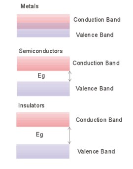 BAND GAPS: The properties of semiconductors are manipulated by
changing the structure of their internal energy levels, which are
spread out into "bands" by the proximity of the component atoms of the
solid. The "valence" band, corresponding to the outermost electrons in
a normal, unexcited atom, is the lowest energy band where electrons
are able to move between ions. However, no net conduction occurs as
long as the band is full. Above this lie the "conduction" bands,
which are not filled, and where electrons will move freely in response
to external EM fields. The separation between the valence and first conduction band
is called the "band gap energy", Eg.
Different materials have a wide range of band gaps. "Conductors" have
a zero gap, meaning that electrons are always available to transfer
charge. "Insulators" have very large gaps, implying zero conduction
except under extreme circumstances. "Semiconductors" have
intermediate gaps.
Absorption of a photon can push a valence electron into the conduction
band and produce a potential electrical signal. The photon energy
must exceed Eg, which implies that there is a maximum
wavelength for excitation given by:
BAND GAPS: The properties of semiconductors are manipulated by
changing the structure of their internal energy levels, which are
spread out into "bands" by the proximity of the component atoms of the
solid. The "valence" band, corresponding to the outermost electrons in
a normal, unexcited atom, is the lowest energy band where electrons
are able to move between ions. However, no net conduction occurs as
long as the band is full. Above this lie the "conduction" bands,
which are not filled, and where electrons will move freely in response
to external EM fields. The separation between the valence and first conduction band
is called the "band gap energy", Eg.
Different materials have a wide range of band gaps. "Conductors" have
a zero gap, meaning that electrons are always available to transfer
charge. "Insulators" have very large gaps, implying zero conduction
except under extreme circumstances. "Semiconductors" have
intermediate gaps.
Absorption of a photon can push a valence electron into the conduction
band and produce a potential electrical signal. The photon energy
must exceed Eg, which implies that there is a maximum
wavelength for excitation given by:
| Material | Eg(eV) | Lammax (Å) |
|---|---|---|
| Pure Si | 1.1 | 11,300 |
| GaAs | 1.43 | 8,670 |
| InSb | 0.36 | 34,400 |
| Hg1-xCdxTe | 1.55x | 8,000/x |
DOPING: The "elemental"
semiconductors are those elements in group IVa of
the Periodic Table
(including Si and Ge). These have four electrons in their valence
shells, half the maximum allowed. These are shared among the ions in
"co-valent bonds." There are many other types of "compound"
semiconductors, however, composed for instance of atoms from group
IIIa and Va of the Table; two of these are listed in the table
above.
The electrical properties of pure semiconductors can be dramatically
altered by adding ("doping with") small amounts (~1 part in
106) of an impurity. The result is called an "extrinsic"
semiconductor.
|
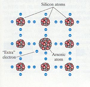
n-type doping 
p-type doping 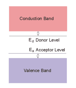
Doping affects energy levels |
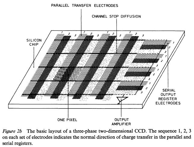
V. BASIC CCD DESIGN
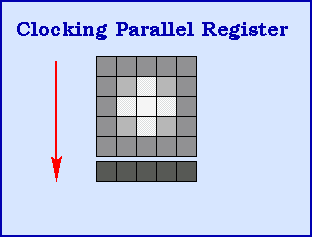
Apart from sensitivity, the key design issues for solid state arrays are to localize photon-produced charges on their surfaces and then arrange to amplify and read them out without distorting the image or introducing unacceptable amounts of noise. A CCD is a charge-transfer device. Its storage, transfer, and amplification electronics are all fabricated on a single piece of silicon. During an exposure, it traps released photoelectrons in small voltage wells. After the exposure, the electrons are shifted in a series of "charge-coupled" steps across the CCD surface, amplified, read out of the CCD, and stored in a computer memory. This is "destructive readout" --i.e. one cannot read the same signal again (unlike other array architectures, where each pixel is coupled to a separate amplifier).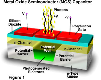
OPERATION SEQUENCE: During exposure
(controlled by a separate shutter), light enters through the
"front-side" electrodes. Photoelectrons generated under the central
electrode will be attracted toward the electrode and held below it.
The corresponding holes will be swept away into the bulk silicon.
Good performance requires little diffusion of electrons away from the
potential well.
|
|
VI. CCD DESIGN ISSUES
CCDs have undergone a long optimization process since 1980. Contemporary designs have excellent performance but still require careful calibration in order to overcome inherent limitations. There is also only a handful of reliable manufacturers of professional-grade chips. Here are some of the issues affecting electronic design and manufacture of CCDs:- INTRINSICALLY LOW BLUE RESPONSE (< 4500 Å):
Caused by absorption in bulk Si and by electrode structures in
"Frontside-Illuminated" chips.
Mitigation:
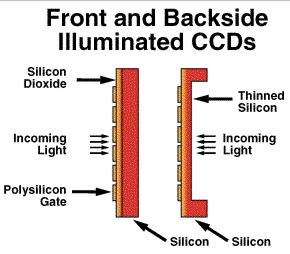
- Use special thin, polysilicon material for electrodes; but these cannot be completely transparent.
- Special Coatings: "Anti-reflection" coatings trap photons, causing multiple reflections as in Fabry-Perot etalons, and therefore enhance absorption. "Downconverter" coatings are phosphors which absorb blue photons but emit green photons at wavelengths where the CCD QE is higher (e.g. "mouse milk," coronene, lumogen).
- "Thinned, Backside-Illuminated" chips: shave off silicon subtrate, leaving only a ~10 µ deep unit and illuminate from backside; greatly improves blue response. The technique was pioneered by Mike Lesser at the University of Arizona.
- Fragile
- Non-uniform thinning
- Surface trapping by SiO2 layer of photo-electrons produced
nearby (shorter wavelengths)
- Interference effects if wavelength ~ chip thickness (i.e. in IR).
Produce strong spatial modulation of response or "Fringing".
Especially serious for terrestrial night sky emission lines. Can be
well calibrated for narrow-band filters or for broad-band filters.
Harder for intermediate band filters.
- Thinning reduces red response. For good response at 5000-10000 Å, thick (~500 µ) front-illuminated chips are preferred.
- CHARGE TRANSFER EFFICIENCY (CTE)
- CTE can be better than 99.999% per transfer from one pixel to the next, but it has to be, since the throughput of a chip with 2048 required shifts = CTE2048.
- It is possible to mitigate the effects of CTE reduction by revising the technical design of a CCD (changing the number of phases or clocking cycles; adding "minichannels") or operationally by adding a pedestal background signal (see below).
VII. ADVANTAGES OF CCD DETECTORS
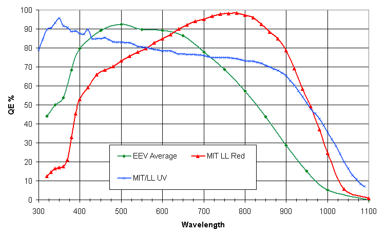
- HIGH QUANTUM EFFICIENCY: Reaching peak values of 80-90% in
the optical band. Much effort was expended to reach these high levels.
Sample response curves for three CCD's from ESO are shown below
right.
- This had tremendous impact on astronomical imaging & spectroscopy. It meant the detection threshold with any instrument was extended 4-5 magnitudes over film and that therefore a 1-m telescope could now pursue the kind of science previously possible only with 4-m class telescopes.
- A key corollary: since we are already near 100% QE, at least in the optical region, achieving significantly lower threshold detections requires larger telescopes rather than better detectors. This was an important factor in the post-1980 rush to build ever larger telescopes. NB: "Quantum yield" can be over 100% for far-UV and X-ray photons -- i.e. more than one photoelectron can be generated but fewer than 100% of photons produce responses.
- LINEAR RESPONSE across the whole range of operation until an exposure approaches full-well capacity (typically 200,000 e/pixel). This allows much improved flux calibrations and much higher precision for flux measurements at all levels than other 2-D systems.
- EXCELLENT DYNAMIC RANGE: Typically 104.
- WIDE WAVELENGTH RESPONSE: Intrinsically sensitive from X-ray to ~1 µ. Arrays based on other materials (e.g. InSb2, HgCdTe) with similar architectures are usable in the IR.
- GEOMETRICALLY STABLE: excellent for astrometry
- ONLY LOW VOLTAGES REQUIRED (~5-15 v)
- RELATIVELY CHEAP, AVAILABLE, SIMPLE compared to other digital 2-D systems. Standard chips cost ~$2-200 K.
- RELATIVELY LOW NOISE compared to many other classes of astronomical detectors, e.g. Pg plates, Reticons, SEC vidicons, etc. Dark current is largely suppressed by cooling. But noise is not negligible. Typical equivalent read noise now is 2-10 e/pixel,
- SMALL PIXELS: typically 10-30 µ. Usually an advantage in devising instrument/detector combinations, but designers should match pixel size to 1/2 of smallest resolvable picture element in the optical system.
- SPECIAL FORMAT/READOUT DESIGNS: By changing electrode structure
and clocking cycles, one can arrange for many different integrate/readout
modes.
-
Rapid clocking/video: inherent in CCDs intended for TV
applications and useful in some astronomical applications
(e.g. speckle interferometry). For bright sources, readout rates of
100 MHz are possible.
Drift Scanning:
-
The basic drift-scanning technique
(Schneider
et al. 1994) is to clock the chip slowly along its
parallel registers while moving the telescope to keep a target
centered on the moving electron cloud as it builds up. The chip is
continuously read out to produce a strip-image of the sky. The
integration time is set by the drift time across the chip.
The simplest approach is to align the CCD parallel registers
east-west, keep the telescope fixed on the sky, and clock the chip
westward at the sidereal rate. A sample application of drift scanning
is
described here.
Drift-scanning is now a standard method for wide-field CCD sky
surveys, most notably the Sloan Digital
Sky Survey
- UBIQUITY: CCDs and other solid-state array devices are now almost universally used in astronomy (amateur & pro). Photographic materials and older electronic detectors have been phased out, except for specialized applications.
- IMMEDIATE DIGITAL CONVERSION OF DATA: The other advantages
of array detectors notwithstanding, it is the immediate conversion of
astronomical signals into a form capable of computer storage/analysis
that has so dramatically transformed UVOIR astronomy since
1980. The practice, pace, & scope of UVOIR astronomy are entirely
different now than in the "photographic" era that preceded widespread
use of CCDs and other array devices. Digital conversion of images and
spectra has enabled quantitative analysis of observations on a scale
not possible before.
-
Among other things, rapid digital processing allows near-real-time
assessment of data and hence much improved use of observing
time---notably in surveys (e.g. for variable sources in MACHO and
supernova searches; moving targets such as asteroids/Kuiper Belt
objects; or combined imaging/spectroscopic surveys such as SDSS,
2dF).
VIII. LIMITATIONS/DISADVANTAGES OF CCD'S
- SMALL SIZE: Individual chips typically are less than 7 cm
square. They cover only a small fraction of the high quality imaging
field on typical modern telescopes. Device size is limited by the small
fabrication yield of large, defect-free chips. The largest routinely
available chips are 4096x2048.
- However, mosaicking technology is now well developed. Typical mosaics are now constructed from 4096x2048 chips.
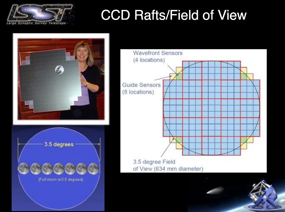
- The largest CCD mosaic camera, containing 201 CCD's, is being built for the Large Synoptic Survey Telescope
- Other examples: (click on images below for enlargements):
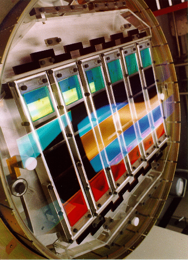
- Sloan Digital Sky Survey: 54 chip mosaic for drift scanning in 5 bands simultaneously
- Canada-France-Hawaii-Telescope MegaPrime mosaic: 40 4096x2048 chips covering 1 degree FOV
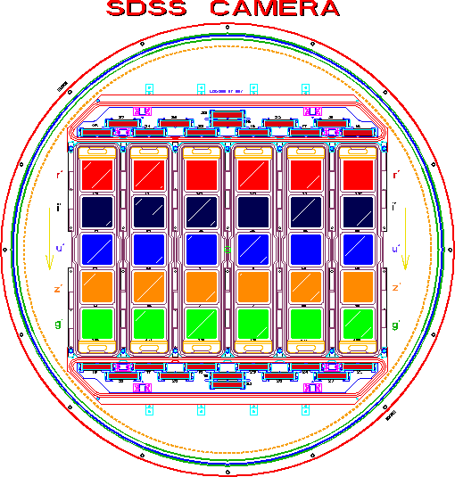
Sloan DSS Camera Sloan DSS Camera CFHT MegaPrime Mosaic
- CRYOGENIC COOLING REQUIRED: To reduce dark noise, cooling to below -100 C is necessary. Thermoelectric coolers are usually not adequate, so cryogens (e.g. liquid N2) are required. Introduces many practical complications. Chips with excellent low-T performance differ from commercial types used at room temperature in digital cameras, cellphones, etc.
- READOUT NOISE: Produced by variations in amplifier gain.
There has been much effort to reduce readout noise, which is now
typically equivalent to 2-10 e/pix.
-
Even at these very low levels, RON can
compromise some types of observations (spectroscopy, surface
photometry), see Lecture 7.
What matters is not the noise per pixel but rather the total noise per
image area, which can extend over many pixels, depending
on the application.
RON effects in some applications can be reduced by using on-chip
binning (see above). In some cases, it may be more advantageous to
use "pulse counting" detectors, which can unambiguously detect
individual photons, rather than CCD's.
- FULL WELL CONSTRAINTS: Bright sources which over-fill pixels can produce "blooming" or "bleeding" along columns, making parts of the chip useless even far from the source. The best solution is operational: e.g. by simply excluding overbright sources or by breaking a long exposure into a series of shorter ones such that saturation is avoided -- and then combining/stacking the result.

|

CCD Flatfield Frame (AAO)

CR's on HST/WFPC2 2400 sec exposure |
- CHARGE TRANSFER EFFICIENCY: Because of "traps" within the CCD's, good CTE is often possible only for signal levels above a threshold of ~10-50 e/pix. For good efficiency at low light levels, this requires adding a "fat zero" (typically 1000 e/pix) electronically or by "preflash" from a diffuse light source. Unfortunately, this also creates added noise (10-30 e/pix). Long-term exposure of CCD's to radiation in space on missions like HST systematically increases the trap density, meaning that CTE reduction is a serious problem there.
- AVAILABILITY HOSTAGE TO COMMERCIAL MARKET: CCD availability has always been driven more by commercial and military applications than science. Scientific CCD manufacture represents only a few percent of the overall $18B array detector market. A serious issue, since "active pixel sensors" (e.g. CMOS devices), a different technology with amplifiers incorporated in each pixel, now dominate the larger imaging array industry. Requirements for good performance at low (astronomical) light levels are considerably different than for room-temperature, short-exposure, mass-produced equipment.
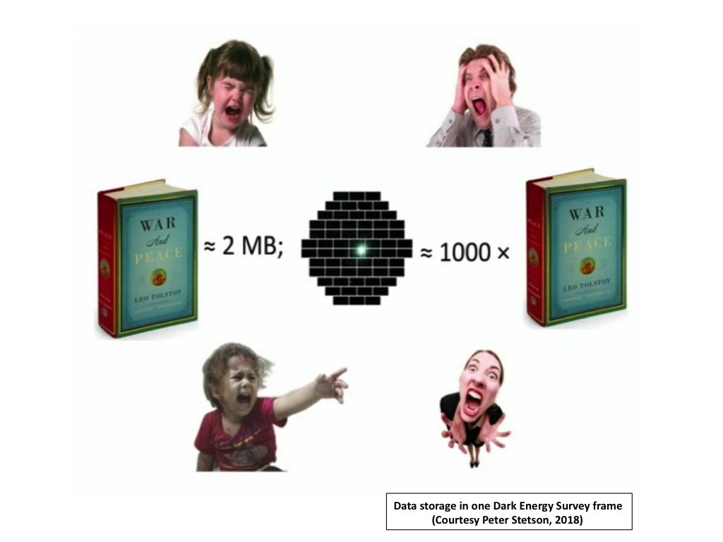
- DATA GLUT! CCDs typically produce 2 x Npix bytes of data per readout, where Npix is the number of pixels. For a 8096x8096 mosaic, this is 130 MB. Data storage/manipulation was a serious problem when CCD's were first introduced, and this influenced the style of data processing systems such as IRAF. Disk and solid-state storage are now much improved, but long-term stability of the massive amounts of data now being produced by array detectors is a non-trivial issue. Cf. the LSST.
IX. EXAMPLE CCD SYSTEMS
- HST WIDE FIELD PLANETARY CAMERA 2 (1992)
- 4 CCD's, optically mosaicked with beam-splitter
- Loral 800x800, 15 µ pixel chips
- Front-illuminated, lumogen phosphor coating for UV response
- RON 5 e/px; QE (6000 Å) 35%
- 4 CCD's, optically mosaicked with beam-splitter
- SLOAN DIGITAL SKY SURVEY (1997)
- Drift scanning mosaic (not contiguous) containing 54 chips
- Tektronix/SITe 2048x2048, 24 µ pixel chips in 5x6
array; for simultaneous broad-band photometry. Both frontside and
thinned backside with AR coating. QE (6000 Å) ~60%; RON < 5
e/px
- Tektronix/SITe 2048x400, 24 µ pixel chips; for astrometry & focus check. Frontside illuminated, RON < 15 e/px.
- Drift scanning mosaic (not contiguous) containing 54 chips
- HST WIDE FIELD CAMERA 3 (2001)
- 2 CCD's, physically mosaicked, contiguous
- Marconi 4096x2048, 15 µ pixel chips
- Thinned, back-illuminated; anti-reflection coating for enhanced blue/UV
response
- Minichannel for improved CTE
- RON 3 e/px; QE (6000 Å) 70%
- 2 CCD's, physically mosaicked, contiguous
- FAN MOUNTAIN CCD SYSTEM (Gen II)
X. CCD HIGH PRECISION CALIBRATION PROCEDURE
A. DATA REQUIRED
- Bias frames
- Dark frames (optional)
- Flat field frames
- Sky flat/fringe frames (optional)
- Flux calibrator fields
- Target frames
B. REDUCTION AND DATA-TAKING PROCEDURES
- SUBTRACT BIAS FRAME: Bias frames (zero exposure time) are
taken with the chip unexposed to light. These measure the electronic
pedestal of the chip. For high precision, average many bias frames,
before and after observations. Check for bias drift during the night.
With some chips, you can determine the electronic bias level from the
"overscan" region on the chip.
- Optional: SUBTRACT DARK FRAME: Median filter many long (~30 min) dark exposures; note possible LED activity of CCD electrodes. Scale result to integration time of each data frame before subtracting.
- DIVIDE BY TWILIGHT OR DOME FLAT FIELD: This removes the
residual pixel-to-pixel variations (typical 5%). Make exposures of
the twilight sky (good diffuse source, but tricky to get exposure level
right; only 2 chances per night). Or make many exposures of diffusely
illuminated screen in dome (disadvantage: often not uniformly
illuminated). Must be done for each filter used because of
color sensitive effects.
-
[Note: photon statistics must yield a SNR significantly in excess of
the final desired SNR -- i.e. if you want SNR = 100, the net
flat field image must contain well over 10,000
photons per pixel.]
- Optional: SUBTRACT SKY FLAT/FRINGE FRAME: Remove night sky emission line fringing effects (worse in near-IR) by observing an uncrowded field in the night sky. Take several exposures, moving telescope by, say, 25 arc-sec between them. Use the "adaptive modal filter" technique to zap star images and create a mean sky frame. Scale to target frames and subtract. Resulting flat field as good as 0.1% can result. A sky flat determined this way is needed for each filter.
- TARGET FRAMES: USE MULTIPLE OFFSETS, DITHERING OR DRIFT SCANNING: For faintest possible photometry, use the multiple-offset exposure technique -- e.g. 500 sec exposures shifted by about 20 arc-sec each -- to reduce flat field errors and identify cosmic rays. You always want more than one exposure anyway for "reality checks" and empirical determination of photometric errors and transient effects.
- REGISTER AND COMBINE TARGET FRAMES: Re-register the offset frames to sub-pixel accuracy (using, e.g., "Drizzle" softare), creating an image "stack."
- REMOVE COSMIC RAY EVENTS: Median filter the signals in each pixel in the stack. Outlying signals caused by cosmic rays and other transients are thereby rejected from the combined image. You must track the remaining "good" exposure time for each pixel.
- COSMETIC TREATMENT: trim off the "lost" parts of the image. Depending on the application, you can interpolate over or mask out bad pixels.
- CALIBRATE FLUX SCALE: Observe "standard stars" in recommended CCD calibrator fields (e.g. star clusters) to determine nightly atmospheric extinction and telescope throughput. No need to take on non-photometric nights (e.g. variable clouds), but no flux calibration for those, either. Calibrator stars should overlap targets of interest in color. These frames are reduced exactly like target frames, apparent fluxes extracted, and the multiplicative factors needed to convert to true fluxes of targets are obtained.
- APPLY GOOD PHOTOMETRIC REDUCTION SOFTWARE: for source IDs,
flux measurements (point or extended source).
=====> RESULT : PHOTOMETRIC CALIBRATION GOOD TO 0.005 MAG
XI. EXAMPLE SCIENTIFIC APPLICATIONS OF HIGH PERFORMANCE CCDs
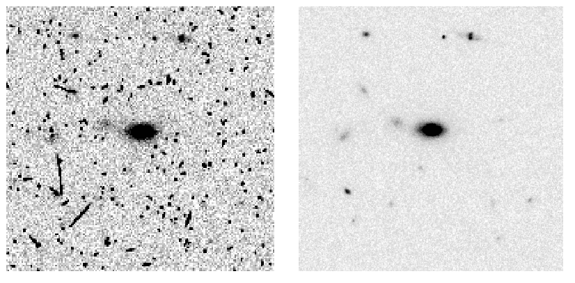
- Deep imaging using subpixel registration. This example employs dithered HST imaging and A. Fruchter's "drizzling" technique. See the image pair below. On the left is one original frame (I-band, 2400 sec exposure). Most of the "features" in this image are cosmic ray tracks, not cosmic objects. On the right is the result of drizzled processing of 12 such frames. The combined image has a limiting magnitude of I ~ 28. It would be impossible to reach such levels with photographic plates or other less-stable and calibrateable systems..
- Color-magnitude diagrams. An example of the improvement
offered by CCD's over photographic photometry in a CMD for the
globular star cluster 47 Tuc is shown below. On the left is a 1977
state-of-the-art CMD based on widefield photographic images with
photoelectric calibrations (Hesser & Hartwick, 1977). On the right is
a 1987 CMD derived from 4-m CCD photometry (Hesser et al. 1987). The
greatly improved photometric precision reveals new features of
astrophysical interest: e.g. the thinness of the main sequence near
turnoff, which places strong limits on the range of ages present in
the cluster, and the shape of the subgiant and asymptotic giant branches.
(Later, yet higher precision, CCD imaging with HST in the
near-ultraviolet bands revealed the existence of multiple populations
with similar ages but different metal and He abundances in many
globular clusters.)
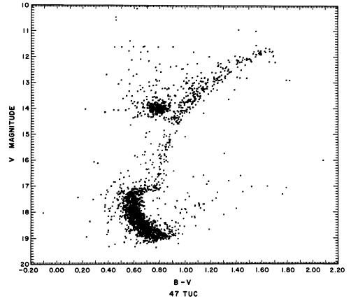
Photographic CMD

CCD CMD
- High precision stellar photometry with Kepler. The Kepler
spacecraft searched for exoplanet transits of 10-16 magnitude stars
using a 42-chip CCD mosaic camera. To reach exoplanets of Earth size,
the transit method requires extremely high precision photometry, which
is possible in space given the absence of atmospheric interference.
Kepler reached a photometric precision of ~30 parts per million at
12th magnitude --- the best ever achieved in astronomy to that time.
A sample light curve is shown below (note the flux scale):

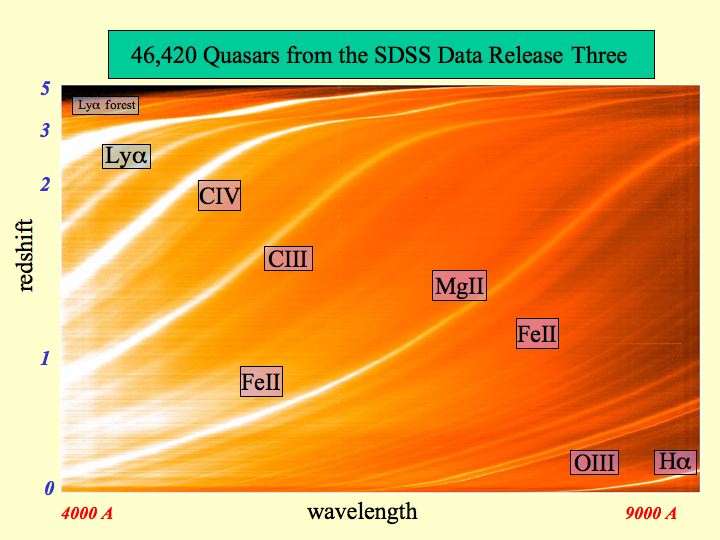
- Multi-object spectroscopy. CCD's are widely used as
detectors in spectrographs. They were the basis for the flourishing
of multi-object spectroscopy, which now extends to the simultaneous
observation of hundreds of sources in a given field. Examples of
these powerful systems are described
in Lecture 10. A sample stack of 46,000
QSO spectra from the first Sloan Digital Sky Survey is shown below.
It would be wholly infeasible to collect such large samples of
astronomical spectra without the powerful capabilities of area
detectors like CCDs.
- High precision astrometry with Gaia. The Gaia space astrometry mission employs a focal plane with 106 specially-designed CCDs fed by two telescopes with different lines of sight and operated in drift-scan mode. To reach its intended limit of ~20 mag, it uses the full 3300-10500 Å band available to the CCDs. It reads data only for selected targets in each field, and each of these is identified by on-board software from a special set of pre-scan mapping CCDs. Gaia achieves an unprecedented precision of about 30 micro-arc-seconds for parallaxes of stars of 15th magnitude.
XII. NON-UVOIR USE OF CCD & RELATED DEVICES
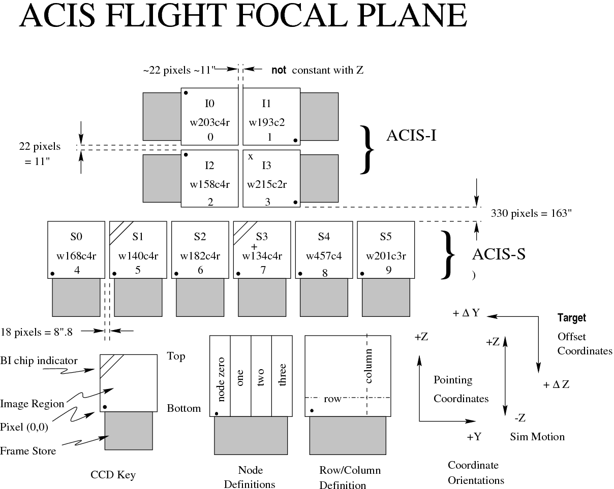
A. X-RAY: CHANDRA/ACIS DETECTOR
-
ACIS is a 10-CCD (1024x1024 chips)
focal plane array used on Chandra for both imaging
and spectroscopy. It uses both back-illuminated and front-illuminated
versions.
It is operated in a pulse-detection mode, unlike the standard
procedure at UVOIR wavelengths.
Each X-ray photon releases more than one electron in the
CCD, in fact, the mean number released is ~ EXR/3.7 eV.
Since Chandra operates at ~ 5 keV, the average electron cloud
corresponding to one photon has ~ 1000 electrons.
The standard operation sequence is to expose for 3.2 seconds, then
rapidly read out the array in 40 ms. The resulting image is
analyzed by on-board software to catalogue the x,y position and
the pulse amplitude of each valid photon pulse.
Because the pulse amplitude is proportional to the photon energy, ACIS
offers an intrinsic spectral resolution of R ~ 10-50.
A difficulty with the ACIS design is that if more than one photon
strikes the same pixel during the exposure time, the counting
analysis becomes distorted, and the photon flux is underestimated.
This is called "pileup." Fortunately, most X-ray sources are faint
enough that this is not a problem.
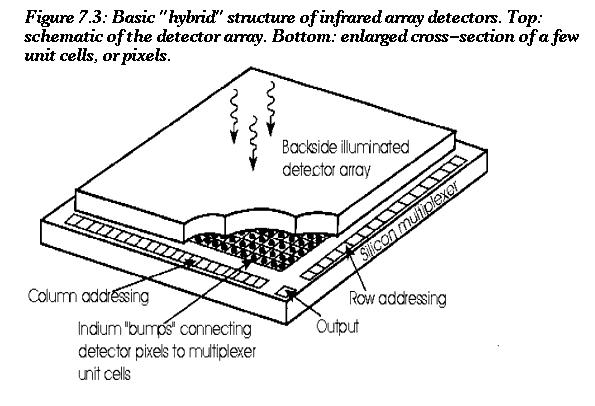
B. INFRARED ARRAYS
-
The table in Sec. IV above shows that pure silicon
photoconductor arrays will not work at infrared wavelengths because of
their large band-gaps, but there are a number of other materials that
will.
There are many varieties of IR detectors in use today. Some of
these are monolithic, i.e. fabricated on single subtrates like
CCD's, and some are
hybrids in which the readout electronics
are fabricated separately from the photon-detection devices.
Hybrids typically use silicon wafers for the readout electronics.
Some actually use CCD-type architecture. The readout is connected to
the photon-sensing material using conducting "bump-bonded" indium
studs. If the wafers ultimately produce readout though a small number
of output amplifiers, they are called "multiplexers" or "MUX's".
Here is
a cross-section of the HST/NICMOS infrared detector, which uses
a HgCdTe ("mercad-telluride") photon detector.

ADDITIONAL WEB LINKS
CCD-World (forum for discussions about CCDs and their use in astronomy) Basics:-
Digital
Imaging/CCD Tutorial at Molecular Expressions
(thorough, elaborate illustrations, but aimed at microscopy)
Britney's Guide to Semiconductor Physics (decorative tutorial)
Semiconductor physics at HyperPhysics (succinct, with many illustrations)
Simon Tulloch Primers on Astronomical Detectors (aimed at advanced amateurs)
-
Sloan Digital Sky Survey CCD Camera
NOIRLab CCD Mosaic Camera Manual
NOIRLab Dark Energy Camera User Guide
ESO Optical Detector Homepage
Status of CCD Development (Steve Holland, LBNL, 2012)
JPL CCD ``Delta-Doping'' Project (for high UV QE)
Scientific CMOS Sensors in Astronomy (Alarcon et al. 2023)
 Previous Lecture
|
 Lecture Index
|
 Next Lecture
|
Last modified April 2023 by rwo
Bandgap images from Britney's Guide to Semiconductors. MOS capacitor illustration from Molecular Expressions. Bucket brigade animation and front/back illumination drawing by C. Tremonti (UWisc). CCD design drawings from C. MacKay, Annual Reviews (1986). Most other images from public observatory sites. Text copyright © 1989-2023 Robert W. O'Connell. All rights reserved. These notes are intended for the private, noncommercial use of students enrolled in Astronomy 511 at the University of Virginia.